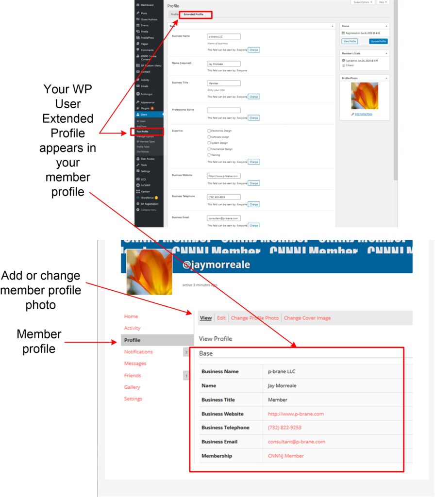
The WordPress User Extend Profile fields are shown in the user’s profile profile page. The fields can be populated as desired. Blank fields are not shown in the user’s profile profile page. User’s can upload their profile photo on this page.
Member Profile Profile
In the illustration below, a member User Extended Profile fields are shown, and where they appear in the member’s profile profile. In the lower part of the illustration, the navigation menu can be seen. This navigation menu enables a member to see their activity, notifications, messages, friends, photo gallery, and settings.
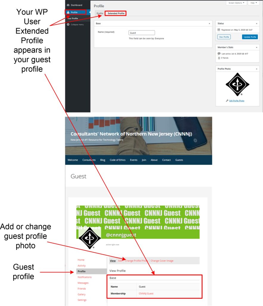
Guest Profile Profile
In the illustration below, a guest User Extended Profile fields are shown, and where they appear in the guest’s profile profile. In the lower part of the illustration, the navigation menu can be seen. This navigation menu enables a guest to see their activity, notifications, messages, friends, photo gallery, and settings.
I have a small business providing electrical system engineering, design, R&D, modeling, prototyping, and networking services. Some of my past projects include an undersea power and communication junction box for an undersea observatory application, fiber optic delay line, an undersea transceiver design study, an actuator driver, and adapting software to control a 6 axis alignment robot.
Before consulting, I worked at AT&T bell laboratories and Lucent Technologies designing undersea telecommunication and optical networking hardware. I co-founded Red Sky Systems which made regional undersea systems.
When I'm not consulting, I study nanotechnology to develop my own products (graphene based terahertz light source). This effort has led to learning Mathematica for modeling device physics and learning to fabricate devices at a nanofab. To learn more, please see my profile on LinkedIn.
